29C3: In-depth analyses of microcontrollers and other chips made easy

At the 29th Chaos Communication Congress (29C3) in Hamburg, Berlin-based security researchers Karsten Nohl and dexter presented a custom-built workstation for "microprobing" semiconductor chips. Comparable in-depth analysis tools such as those for microcontrollers and similar small computer systems often cost several tens of thousands of pounds and have so far mostly only been available in specialised labs. This type of analysis involves examining a chip's individual conductor wires or memory cells with a microscope-like setup and a very thin probe. The "probing device" enables examiners to, for example, record data and command sequences by intercepting bus signals.
Dexter explained that the custom-built workstation consists of a fixed-position microscope that can cope with large working distances to what it is working on, a large magnetic work platform, and a micropositioning system. The micropositioner is a motor-driven stage that can be moved in increments of a few millimetres to a few centimetres. Hardened tungsten needles are required on the microscope's tip to create the electrical contact with the semiconductor material. According to Nohl, who runs Security Research Labs, the overall component cost is no more than €3,000 (approximately £2,440) and will, for the first time, allow interested amateurs to do "microprobing in their basement".
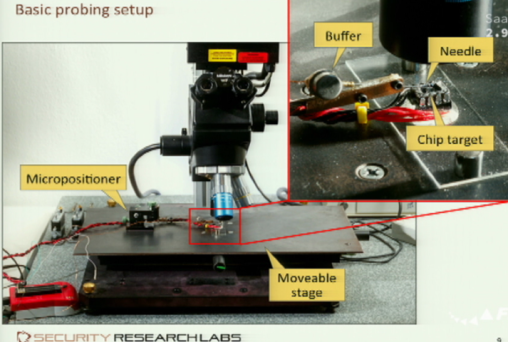
![]() The presented workstation uses a movable stage and micropositioner to place the chip that is to be examined underneath the fixed-position microscope's lens barrel; a tungsten needle is used as a probe
The presented workstation uses a movable stage and micropositioner to place the chip that is to be examined underneath the fixed-position microscope's lens barrel; a tungsten needle is used as a probe
Source: Security Research Labs
Dexter says that he is planning to release the construction plans for the probing device and its parts under an open source licence in the near future. Inexperienced newcomers should start with microcontrollers that are quite old and include few defences against data extractions, he explained. Apparently, cracking open the chip packaging itself far enough to be able to use the device for analysis purposes "isn't easy"; however, the researcher noted that even amateurs can manage it to some degree eventually. Often, softly levering the chip packaging open with a screwdriver is enough to remove anything that may be in the way, dexter explained, adding that the only thing to pay attention to is that the contacts must remain intact. A little hot nitric acid or an ultrasound acetone bath can also help uncover the desired silicon, he added.
The obvious way to start the actual inspection is to capture a detailed image and study the chip's microstructures. Then, the examiner can focus on components such as fuses or the output lines of specific memory areas. Apparently, applying paint to the semiconductor elements can often work wonders because it makes it easier to identify readable transmission pathways.
Going into detail, Nohl explained that software can, for example, be extracted from a chip by overwriting fuses or by performing a linear code extraction – this requires creativity as examiners can, for instance, modify running routines via special commands, perform memory tests, or monitor the launch of an executable program. The researcher noted that all mainstream architectures tend to disclose their memory content with a little manipulation. Nohl said that microprobing is generally relevant when trying to activate a chip's hidden capabilities or detect unwanted backdoors. Ultimately, it increases the security of the devices that are equipped with such semiconductor elements, he added.
Nohl explained that a race between manufacturers and hackers has developed in this area of analysis in the same way as in many other areas of security research. For example, he said that special metal meshing is now being used to prevent microprobing, and that smartcard chips are among those that have been equipped in this way.
However, the security expert said that manufacturers are a long way away from winning the race. By using technologies such as a focused ion beam, clever attackers with the necessary equipment can drill into such protective shields in the top layer. Nohl added that, like scanning electron microscopes, these technologies allow attackers to manipulate chip surfaces in a very controlled way, and lasers or UV radiation can sometimes also be used to achieve similar results. Other hackers work on the back of microcontrollers to directly tap into components such as transistors through the silicon that is applied there, he noted. According to the researcher, any chip that has been shipped in the past few years is vulnerable to this kind of attack.
A video of the presentation is available on YouTube.
(Stefan Krempl / fab)


![Kernel Log: Coming in 3.10 (Part 3) [--] Infrastructure](/imgs/43/1/0/4/2/6/7/2/comingin310_4_kicker-4977194bfb0de0d7.png)

![Kernel Log: Coming in 3.10 (Part 3) [--] Infrastructure](/imgs/43/1/0/4/2/3/2/3/comingin310_3_kicker-151cd7b9e9660f05.png)