Processor Whispers: Of devils and frostbite
![]()
by Andreas Stiller
Intel's next processor generation is casting long shadows, especially in Germany. One can already order Haswell chips online, here and there, but competitor AMD also plans to come up with interesting chips in the course of the year.
At CeBIT in Hanover, Asrock and Biostar showed off numerous boards intended for Haswell, and MSI – in a secluded part of the reseller area – at least produced one board with the Lynx Point chipset Z87 and LGA1150 socket when they were asked about it. In all cases, though, the sockets were empty, unlike at the Embedded World event in Nuremberg, Germany, where, for example, Kontron had exhibited its boards equipped with Haswell processors.
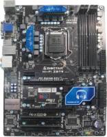
![]() At CeBIT, the Haswell sockets were still empty, like the one on this Hi-Fi Z87W from Biostar.
Ahead of CeBIT, the small German computer company Deviltech from Saxony- Anhalt also blurted specifications about the planned Devil 7700 and Fragbook DTX notebooks, which not only included a few details about the Haswell processor, but also about the yet-to-be-announced mobile graphics chips GTX 770M and 780M from NVIDIA. With a 3DMark Vantage value of up to 29358, these are supposed to be around 30 per cent faster than their predecessors. Intel and NVIDIA were not at all amused about these indiscretions and Deviltech quickly withdrew the press release, but as we all know: what goes online, stays online.
At CeBIT, the Haswell sockets were still empty, like the one on this Hi-Fi Z87W from Biostar.
Ahead of CeBIT, the small German computer company Deviltech from Saxony- Anhalt also blurted specifications about the planned Devil 7700 and Fragbook DTX notebooks, which not only included a few details about the Haswell processor, but also about the yet-to-be-announced mobile graphics chips GTX 770M and 780M from NVIDIA. With a 3DMark Vantage value of up to 29358, these are supposed to be around 30 per cent faster than their predecessors. Intel and NVIDIA were not at all amused about these indiscretions and Deviltech quickly withdrew the press release, but as we all know: what goes online, stays online.
USB 3.0 Issues
Up to now, it seemed certain that the launch would coincide with the Computex in June, but now there are rumours about problems with the Lynx Point chipset (Z/Q/H/QM87...). Only two years ago, the launch of Sandy Bridge was delayed because Cougar Point (H67/P67) had issues with SATA II. This time, with Lynx Point, it's the USB 3.0 ports, which are reported to have problems awaking from the S3 slumber, but Intel still has enough time to fix that with a new stepping.
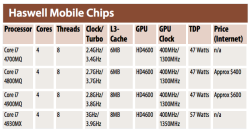
![]() Haswell Mobile Chips
Relevant web sites from the Far East, such as VR-Zone, had already published Haswell's processor names, number of cores, clock speed, TDP and so on a few months ago – thanks to Deviltech's announcement we now know that that information was correct. Intel has partially turned around the endings of the names in comparison to the current Ivy Bridge generation: QM becomes MQ and XM becomes MX. One can already find lots of offers on the internet, too, as a Google search with BX80647I74900MQ or BX80647I74800MX shows.
Haswell Mobile Chips
Relevant web sites from the Far East, such as VR-Zone, had already published Haswell's processor names, number of cores, clock speed, TDP and so on a few months ago – thanks to Deviltech's announcement we now know that that information was correct. Intel has partially turned around the endings of the names in comparison to the current Ivy Bridge generation: QM becomes MQ and XM becomes MX. One can already find lots of offers on the internet, too, as a Google search with BX80647I74900MQ or BX80647I74800MX shows.
At the same clock speed, as revealed, the Haswell architecture is supposed to deliver a performance increase of 9 per cent – not exactly a giant leap for a new processor generation. This figure had also been leaked before: the Russian web site OCLab.ru had released a few pi and prime number benchmark results for some prototypes. However, it's very unlikely that these results take into account the numerous options that Haswell provides with the new AVX2 instructions. Someone will have to write code to make use of them first after all. AMD is one step ahead in this regard, its Piledriver already features Bit Manipulation Instructions (BMI) as well as other extra instructions.
In any case, the focus for the design of the Haswell processor was not such much on performance, but rather on improved energy management. And it will be interesting to see how the new fast wake-up mode S0ix will perform in practice. Experts are at a loss as to how Intel has managed this "from nought to 60 in no time at all".
And as for the formerly much-talked-about Transactional Memory (TSX)? As of yet, the leaked data sheets provide information about various features like Vpro, TXT, VT-d, VT-x and AES-NI, but not about TSX. So this feature will probably remain reserved for the server chip Haswell-EP, which will have up to 14, or maybe 16, cores and is not due until 2014. At least the Xeon E5-1200 V3, destined for a socket in the Denlow platform, is still scheduled for this year.
Its code name slips my mind right now, probably just Haswell-EN. Should you at some point find yourself confused by all the code names: Intel has listed and linked all contemporary code names for processors, chipsets, boards, servers, network chips and SSDs in a clearly arranged layout at ark.intel.com under "Products by Code Name". The listed processor names alone, from Arrandale to Yorkfield, give a total of 76, among them some that are unheard of, like Gladden (a Sandy Bridge chip), which is not even mentioned in Wikipedia's extensive "List_of_Intel_Codenames". But then Wikipedia's list also contains the names of chips that, embarrassingly, never made it to the market, like Tejas, Timna and Larrabee.
APUs for Frostbite
At Computex in June, AMD will presumably present the tablet chip Temash as a small counterpoint to Haswell, and maybe it will also show off the somewhat more powerful Kabini for notebooks. At least these chips are officially scheduled, with up to four Jaguar cores, for the first half of the year. And something else is now official too: the application of AMD APUs with eight Jaguar cores in Sony's PlayStation 4. But there is also unofficial news, namely that AMD plans to derive and market a PC-optimised version without any special Sony IP.
Game developers, like the ones responsible for Frostbite, the game engine from Digital Illusions CE that drives, among other games, Battlefield, have meanwhile tweeted images of development systems with "Next-Generation APUs". It is quite possible that we are dealing with the Kaveri chip with Steamroller cores and Graphics Core Next (GCN) here. Their shared-memory model offers many, as yet unknown possibilities for the interaction between CPU and GPU. In order to take advantage of this, lots of code will have to be rewritten, so the earlier the developers receive prototypes, the better.
(djwm)


![Kernel Log: Coming in 3.10 (Part 3) [--] Infrastructure](/imgs/43/1/0/4/2/6/7/2/comingin310_4_kicker-4977194bfb0de0d7.png)

![Kernel Log: Coming in 3.10 (Part 3) [--] Infrastructure](/imgs/43/1/0/4/2/3/2/3/comingin310_3_kicker-151cd7b9e9660f05.png)